

TSMC's Latest Japan Announcement Shows its Increasing Savvy
[Opinion] Adding 3nm to the Kumamoto site is more than altruism, it's a pragmatic adjustment to a changing market. The timing was no mistake, either.

Good Afternoon from Taipei,
TSMC CEO CC Wei delivered a fabulous pre-election gift to Japanese Prime Minister Sanae Takaichi on Thursday by announcing the addition of 3-nanometer technology to the company’s Japan venture.1
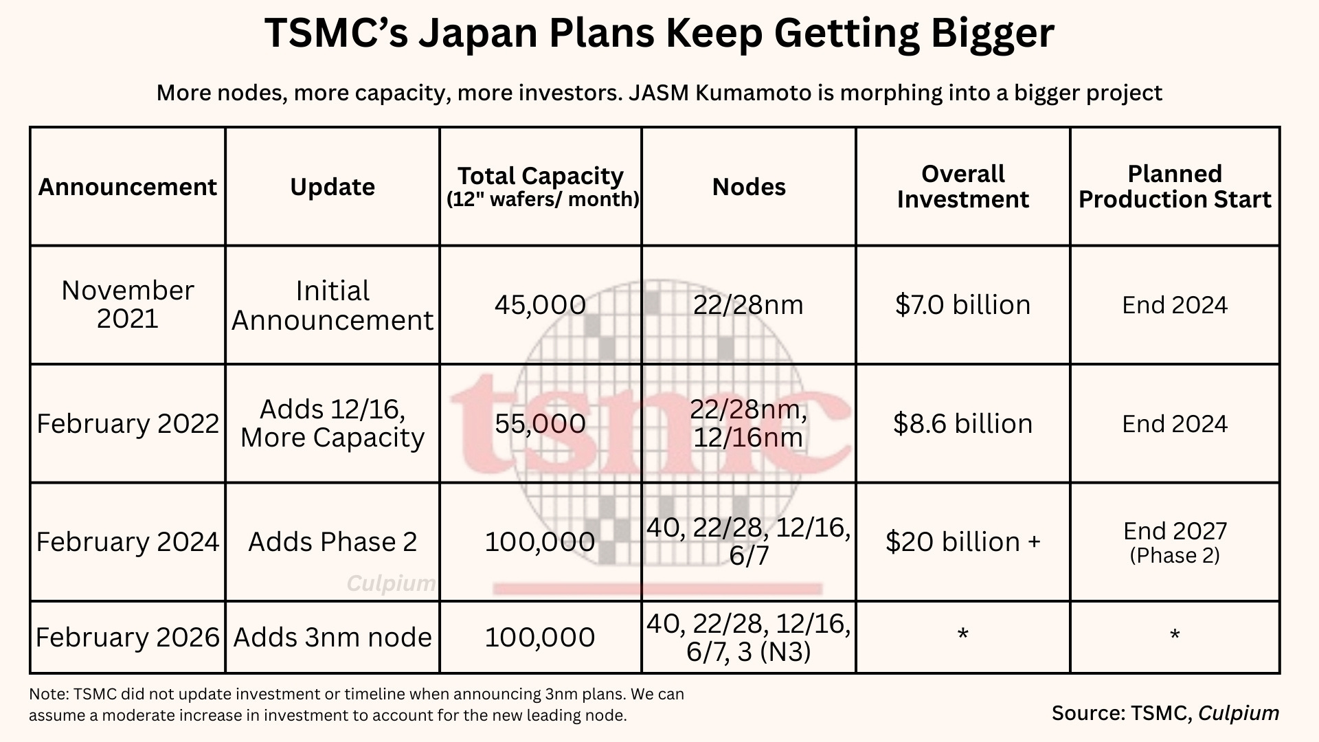
The formation of Japan Advanced Semiconductor Manufacturing Inc. was first announced in November 2021 as a joint venture in which Sony Semiconductor Solutions Corp. would take a stake of up to 20%. Plans at the time were modest: a $7 billion investment with 22/28nm technology, and monthly capacity of 45,000 wafers per month “to address strong global market demand for specialty technologies.”
Fab 23 in Kumamoto has since grown in size and scope. More nodes, more capacity, more investors and a second phase have since been added. The project’s importance has grown so much that Taiwan’s China Airlines and Starlux Airlines commenced direct Taipei-Kumamoto flights in 2023.
The addition of vehicle-components maker Denso to the shareholder table saw more talk of automotive semiconductors, which became a hot topic during the Covid-era chip shortage. Jon at Asianometry produced a timely video in the midst of this saga which pointed out that older semiconductors have been a bigger issue in the supply-demand imbalance than leading-edge capacity. JASM’s plans — centered around 40nm through 12nm nodes — were part of a long-term strategy to address this issue.
The term HPC (high-performance computing) started sneaking into discussions of Kumamoto only in the last two years as this second phase was added. But Japan is not a player in HPC more broadly, nor in AI chips specifically — which are a subset of HPC. The 6/7nm technology has been in the mix since Phase 2 was announced, but there was never any sense that this node — the first to use EUV — was a major driver of the project.
Booming demand for AI GPUs has led to progressively louder allegations that TSMC failed to expand quickly enough, and is thus holding back America’s AI dream. Jon and Stratechery’s Ben Thompson have been duking it out over whether or not it’s fair to blame TSMC, with successive videos and newsletters outlining their positions. I see Ben’s point, from a US-centric perspective, but come down on the side of viewing these complaints as a little unfair and out of touch with the realities of semiconductor capacity investments.
I doubt TSMC Chairman and CEO CC Wei is listening to Ben, Jon or myself, but he is listening to Jensen Huang and Lisa Su, while also maintaining a solid relationship with Tim Cook. As Culpium outlined in exclusive coverage of those discussions, Wei delivered a price rise to Cook back in August just as Apple finds itself in the unfamiliar position of having to scrounge for TSMC capacity amid Nvidia’s rise to the top of the client table.

Wei’s gift to Takaichi on Thursday February 5 — three days before Japan’s snap parliamentary elections — are a reflection of the Taiwanese executive’s savvy pragmatism.
TSMC has known about its plans to add 3nm to Kumamoto for at least a month or two, according to my sources. A conspiracy theorist might conclude that he chose the week prior to Takaichi’s bid for re-election to announce this news— directly to her face — as a political move. A more nuanced take would posit that he was too busy closing out 4Q and announcing results, while managing the world’s sixth-largest company, to worry about giving face to a foreign leader.
There’s probably elements of both. Here’s what TSMC said:
Dr. C.C. Wei, Chairman and CEO of TSMC, stated on February 5 during a meeting with Japanese Prime Minister Sanae Takaichi that TSMC is now planning to use 3nm process technology for production at JASM's second fab, currently under construction in Kumamoto, to meet strong demand driven by AI. Dr. Wei also expressed his appreciation for the continuous support of the Japanese central government, Kumamoto Prefectural Government, Kikuyo Town Government and the local community, and believes Japan’s forward-looking semiconductor policy will deliver significant benefits to the semiconductor industry
— TSMC statement to Culpium, 6 February 2026.
Note the reference to meeting “strong demand driven by AI.”
This move — which adds the potential for 50,000 wafers of monthly 3nm capacity to TSMC’s global footprint — achieves two more important goals than pandering to foreign politicians.
The first is to soak up Kumamoto capacity at a time when, according to my sources, demand at the fab from the automotive and specialty-chip sectors appears to be weaker than previously expected. JASM is not particularly big by capacity or revenue standards, but is symbolic of TSMC’s overseas expansion. The facility was built and ramped far more quickly than its Arizona site, a function of a more-similar industrial and work culture between Japan and Taiwan than the US and Taiwan. For all intents and purposes, JASM was looking like a great success. Having utilization fall too low would challenge this narrative, even if only internally.
Second, TSMC’s ability to add new leading-edge capacity is constrained by multiple factors including land availability, and construction & equipment-install times. Each node tends to build on the prior one, in terms of both process and tooling. Since EUV was already slated for Fab 23 Phase 2 as a function of 6/7nm being on the roadmap, it’s not a huge stretch to add 3nm and thus quickly add more volume for making AI chips.
I doubt many of these wafers will be going to Japanese GPU designers — if you know any, please email me. In fact, they’ll likely be popped on a Starlux or China Airlines jet and get deposited back in Taiwan for CoWoS packaging, at which point the names Nvidia, AMD, or Apple will be stamped upon them.2
Everybody wins. TSMC gets to soak up some Kumamoto capacity and the GPU players get more volume more quickly for AI chips, while on Sunday we’ll find out whether Takaichi is also a winner. And who knows, maybe the naysayers will start bitching just a little less about TSMC’s “failure” to expand leading-edge capacity quickly enough.
Thanks for reading.
More from Culpium:


Technically its N3, a label somewhat divorced from the 3nm measurement used to describe the size of interconnects.
Apple isn’t using CoWoS (yet) but uses the InFO advanced packaging solution better-suited for mobile processors.
Nice post. Thank you.
I read the announcement to mean that Fab23 (JASM) P2 would be N3, rather than the originally announced 6nm/7nm.
I didn’t think what was announced in the meeting with PM Takaichi would be a new P3 for the JASM fab. Or did I misread?
I was interpreting the 2021 and 2024 announcements as both being for Fab23 P1.
When I visited in May 2025, there was definitely only one fab.
Thanks for reading.